Antenna integration into a device is not all about selecting the correct antenna. Bad antenna integration will completely ruin the functionality and render wireless communication unreliable and feeble. The engineers have to be very cautious in PCB layout, antenna tuning, and rigorous testing to ensure the antenna operates in optimal conditions. We here present the best practices in antenna integration with practical guidelines on wireless performance maximization in devices.
PCB Layout and Routing
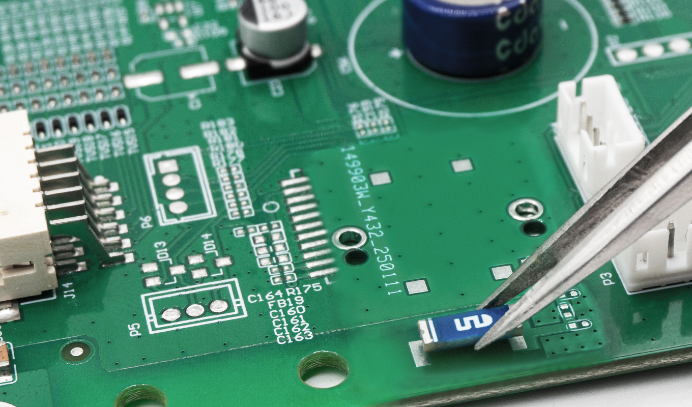
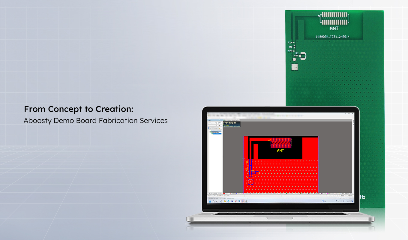
The design of the PCB is an important factor in the performance of an integrated antenna. The proper placement of the antenna and right-optimized routing have a major role in the efficiency with which the antenna will receive and send the signal.
Key considerations for PCB layout include:
- Antenna Placement: Leave sufficient room around the antenna so it will not be disturbed with the nearby parts. Metal components such as power lines, the chassis, or other PCB traces have the possibility to disturb the antenna heavily through signal reflection or blocking. The rule of thumb is to leave at least 10mm of clearance around the antenna on the PCB.
- Ground Plane: The ground plane should be big in size in order to provide the signal from the antenna with the correct reference. Too small ground plane reduces the antenna’s gain, but noise or signal distortion is created if the plane is too big in size. To have the optimal performance, make the ground plane not less than 1.5 times the antenna’s size.
- Impedance Matching: One of the most important factors in antenna performance is impedance matching. Antennas typically require a 50-ohm impedance transmission line. Maintaining this impedance throughout the PCB ensures maximum power transfer with minimal signal loss. The trace width and spacing must be carefully calculated based on the PCB material and the desired impedance.
For example, a PCB designed with FR4 material and a thickness of 1.6mm might require a trace width of around 1.2mm to achieve a 50-ohm impedance. Deviations in this can cause mismatches that lead to reflections and signal loss.
Antenna Tuning
After the PCB layout is done, you need to tune the antenna to account for how the antenna interacts with the device’s environment. Things like what the device is made of, its shape, and the placement of nearby components (like metal enclosures) can influence the antenna’s resonant frequency and overall performance.
Key steps in antenna tuning include:
- Adjusting the Frequency Response: Different enclosures and materials may detune an antenna through a change in resonant frequency. The problem may be resolved with the use of matching circuits with inductors and capacitors incorporated in the circuits. They help realign the resonant frequency of the antenna back into the optimal frequency.
- Network Tuning: Capacitors (C) and inductors (L) are the primary components employed for the tuning of an antenna. They allow for the impedance and resonance adjustments of the antenna and hence its alignment with the target frequency. For instance, an impedance matching network typically uses an L-C series combination to correct frequency deviations caused by the enclosure.
- Using a Network Analyzer: After the antenna adjustment, it is recommended to use a network analyzer to measure the reflection coefficient (S11). A low value for S11, preferably below -10 dB, indicates the signal is effectively coupled into the antenna with little reflection. The fact indicates the antenna is resonating on the desired frequency.
Tuning the antenna is very important for IoT devices. This is because the antenna’s performance can change a lot depending on the surrounding components or casing. For example, a plastic casing may not change how well the antenna works. But a metal case can shield or detune the antenna.
Testing and Validation
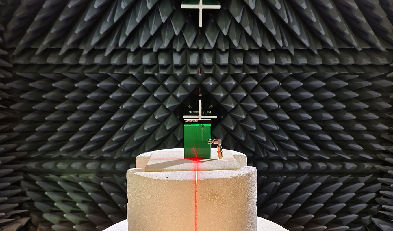
While PCB layout and antenna tuning are essential, the final step in antenna integration is testing. OTA (Over-the-Air) testing is a critical process that helps validate antenna performance and verify that the device performs as expected in real-world conditions.
Key testing procedures include:
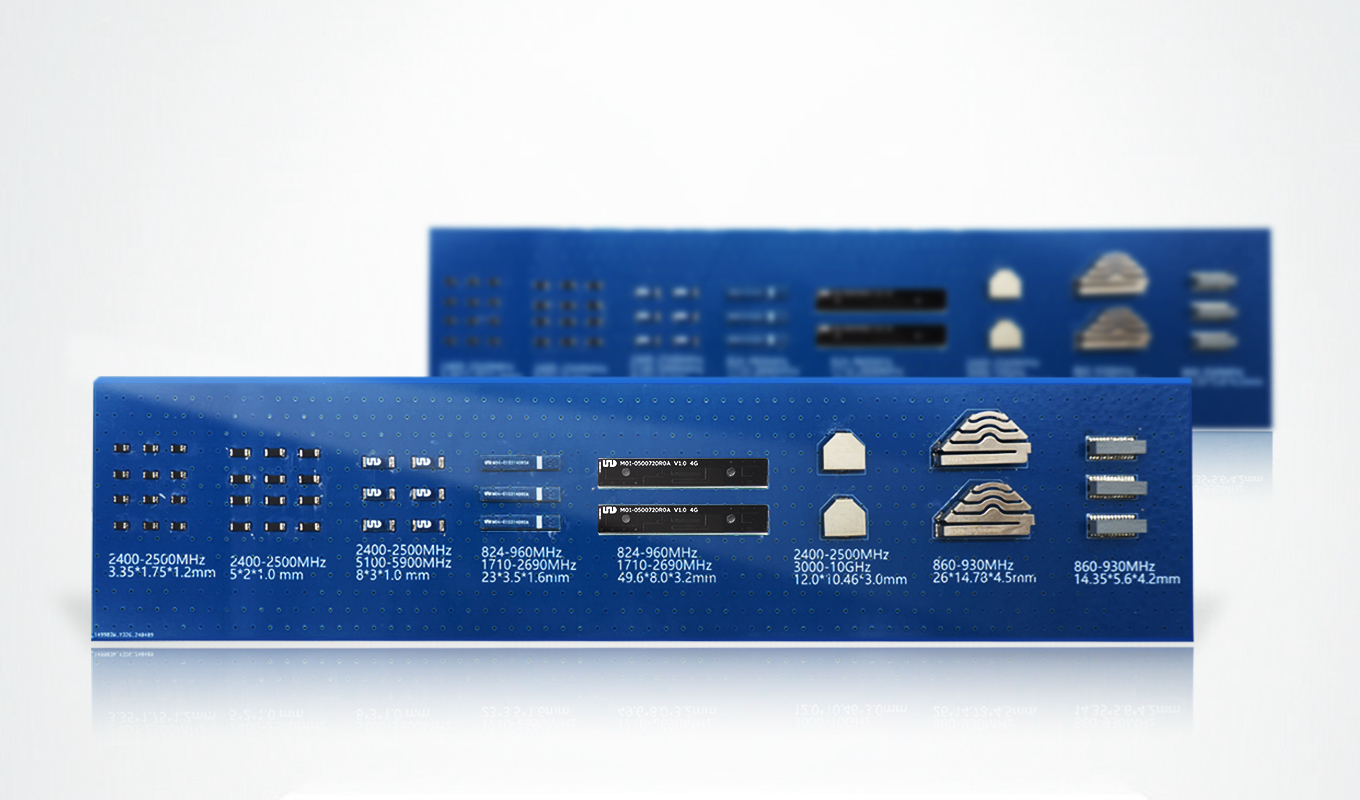
- Antenna Gain Measurement: The gain of the antenna should meet the design specifications. Antenna gain is a measure of the antenna’s ability to focus the radiated energy in a particular direction. A typical goal for wireless devices is a gain of around 2-4 dBi, depending on the application. The measurement should be taken in an anechoic chamber, where external noise and reflections are minimized.
- Radiation Pattern: The radiation pattern of the antenna describes the distribution of radiated energy in space. During testing, verify that the radiation pattern is symmetrical and does not show significant distortion, which may indicate integration issues. For example, a distorted pattern can occur if components within the device block the antenna’s signal path.
- Impedance and Efficiency Testing: Impedance mismatch can lead to inefficient energy transfer. Measure the antenna’s impedance across its operating frequency range to ensure that it remains consistent with the target impedance. For best performance, aim for a VSWR (Voltage Standing Wave Ratio) of less than 2:1 across the entire operational bandwidth.
- Environmental Testing: In addition to testing in an anechoic chamber, perform tests that simulate real-world environments. Place the device in various orientations and test it in multiple environments (e.g., different temperatures, humidity levels, or under various operational conditions). This will help ensure that the antenna performs consistently across different scenarios.
Checklist for Successful Antenna Integration
To streamline the antenna integration process, here’s a checklist for engineers:
| Step | Best Practice |
| 1. PCB Design |
|
| |
| |
| 2. Tuning the Antenna |
|
| |
| 3. Testing and Validation |
|
| |
| |
|
Following these practices not only guarantees optimal wireless performance but also minimizes potential delays and post-production modifications, helping engineers create successful and efficient devices.
For additional support, Aboosty’s team offers specialized expertise in RF testing, PCB design, and antenna integration. Our services can help engineers optimize antenna performance, avoid costly redesigns, and reduce time-to-market for wireless products.