.jpg)
Best Placement Tips for Embedded Antennas
Where to place your antenna for optimum performance?
Application Solution
Aboosty Technology (also known as, Seeed Studio) is an innovative IoT technology company, which specializes in hardware research, production and sales for edge computing, network communication, and smart sensing applications. Moreover, the company provides a wide variety of R&D support and services for customized products.
With Shenzhen’s vast resources, and trusted technology and distribution partners around the world, Aboosty strives to be the most integrated platform for creating hardware solutions for IoT, edge AI applications.
- Application Solution link 01
- Application Solution link 02
- Application Solution link 03
- Application Solution link 01
- Application Solution link 02
- Application Solution link 03
- Application Solution link 01
- Application Solution link 02
- Application Solution link 03
- Application Solution link 01
- Application Solution link 02
- Application Solution link 03
- Application Solution link 01
- Application Solution link 02
- Application Solution link 01
- Application Solution link 02
- Application Solution link 03

Introduction
Today circuit boards get smaller and more compact while component densities increase, thanks to the trend to miniaturize wireless communication devices. Although this shift to miniaturized technology has benefited many areas of electronic design, it constrains RF front-end design. Finding sufficient space for an antenna becomes more of a challenge for RF engineers.
Why Antenna Placement Matters
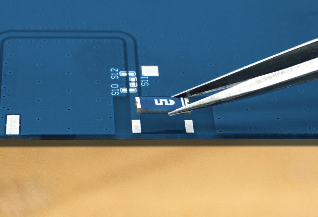
The placement of an embedded antenna on a printed circuit board (PCB) is paramount, as it significantly influences the performance of devices. Efficient signal transmission and reception are essential for the reliability and functionality of wireless systems, while optimal antenna mounting accelerates the realization of these.
Before designing wireless devices, designers must choose the right type of antenna. SMD chip antennas are small, cost-effective, and easy to integrate, making them ideal for compact devices. For more complex designs, flexible Printed Circuit (FPC) antennas are a viable alternative. FPC antennas are flexible and can be positioned around the contours of a device, maintaining high performance even in intricate designs.
When placing the antenna, engineers tend to reduce the space allocated for the antenna’s ground plane. Nevertheless, even a small drop in the ground plane size can make a huge difference in performance at sub-GHz frequencies. The positioning of an embedded antenna on a printed circuit board (PCB) is therefore a critical factor that can significantly influence the performance of the device.
It is essential to account for space on the PCB, position, clearance, the ground plane, and correct connection to other components when placing an antenna. Getting these aspects right before you start the design will help to achieve a successful launch with reliable wireless performance.
Position Antennas at the PCB Edge
Generally, antennas should be placed at the edge of a circuit board away from other circuit components to maximumly minimize electromagnetic interference. The aim is to keep the antenna away from noise-generating components such as power ICs, clocks, and other signal buses. Ensuring adequate clearance from these components helps maintain signal integrity and improve overall performance.
Three Ways to Mount the Embedded Antenna
Placing the antenna on the PCB corner is generally the most desirable location. This typically results in better antenna gain.
Placing the antenna at the side edge of the PCB can also ensure the best performance. Some antennas reach their highest performance when paling on the long-side edge of the circuit board, while others achieve the best results when positioned on the short-side edge of the board. Antenna designers need to experiment to find the best answer.
In extreme cases, the antenna may be placed over or between ground planes. In this case, Antennas should not be placed directly above any ground layers on the PCB, or the metal layer or battery beneath would affect how signals are propagated, disrupting the antenna’s functionality.
More Practicle Tips for Perfect Antenna Mounting
With Shenzhen's vast resources, and trusted technology and distribution partners around the world, Aboosty strives to be the most integrated platform for creating hardware solutions for IoT, edge AI applications.
With Shenzhen's vast resources, and trusted technology and distribution partners around the world, Aboosty strives to be the most integrated platform for creating hardware solutions for IoT, edge AI applications.
With Shenzhen's vast resources, and trusted technology and distribution partners around the world, Aboosty strives to be the most integrated platform for creating hardware solutions for IoT, edge AI applications.
With Shenzhen's vast resources, and trusted technology and distribution partners around the world, Aboosty strives to be the most integrated platform for creating hardware solutions for IoT, edge AI applications.
More Practical Tips for Perfect Antenna Mounting
Adhere to the demo board to match the datasheet performance
The reference board serves as an easy template, saving engineers significant time and effort. By following the demo board design as closely as possible, engineers can effectively address factors for chip antennas, such as PCB dimensions and ground plane sensitivity. Data sheets will outline PCB board details for each antenna.
Of course, it’s not always possible to follow the reference board exactly. In such cases, be sure to follow the other principles of best antenna placement in this article.
Prevent metal enclosure coverage
When placing the antenna in an enclosure, ensure that the antenna is not completely covered by the metallic casing/housing/enclosure, especially in compact designs where space constraints may lead to suboptimal placement. Metallic housing can severely affect the impedance and overall performance of the antenna. Right antenna exposure is critical to maintaining signal quality and successful antenna placement.
Minimize interference
1) In the special case of multi-layer PCBs, pay attention to avoiding overlapping ground planes.
Metal layers under the antenna can interfere with signal propagation and reduce functionality. Refer to the antenna’s data sheet for recommended clearances to ensure that the antenna is placed correctly to avoid overlapping with the ground plane.
2) Coexistence of antennas
In devices with multiple antennas, achieving effective isolation and correct orientation is essential due to the antennas’ sensitivity to their surrounding environment. To minimize interference and preserve signal integrity, antennas operating in similar frequency bands should be separated as widely apart as possible and oriented at 90-degree angles to each other.
Leave extra space for the antenna’s matching network
In the design and development of a product, it is vital to allocate extra space for necessary impedance adjustments without compromising performance.
Matching networks are implemented as close to the load or source as possible, as the length of the feedline will affect impedance matching and power transfer. The three aspects of the antenna, impedance matching network, and radio output should be placed proximity close to each other to ensure a low signal loss from chip to antenna.
Dimensions of the Ground Plane, Radiation Patterns, and Circuit Board Shape
Dimensions of the Ground Plane
Enough space for the ground plane is a crucial factor in antenna performance. Adhering to datasheet recommendations for ground plane dimensions ensures adequate support for the antenna. In constrained spaces, consider alternatives like Flexible Printed Circuits (FPC) or case-mounted antennas.
Radiation Patterns
Each antenna features a unique radiation pattern that dictates its ideal placement. Understanding and utilizing this pattern is essential for maximizing performance. Consult the datasheet for specific placement recommendations based on the antenna’s radiation characteristics to find the most effective antenna orientation.
Circuit Board Shape
The shape of the circuit board impacts antenna placement. Antennas designed for corner placements might not be suitable for circular or irregular boards, for instance, circular boards can not meet the requirement of mounting the antenna on a corner. RF engineers need to adjust placement strategies to suit the specific shape and layout of the circuit board to achieve the best placement for the antenna.

Conclusion
In summary, optimal embedded antenna placement is critical in wireless designs. Following these suggestions, designers can ensure efficient antenna operation, delivering robust and reliable wireless communications.
Follow our latest news


Tool.ABOOSTY
ABOOSTY has developed a free antenna selection and placement tool for global designers and engineers working with wireless technology.
